Fermi Energy Level In Semiconductor : Why Should The Fermi Level Of A N Doped Semiconductor Be Below The One Of A P Doped Physics Stack Exchange - The fermi energy is described as the highest energy that the electrons assumes at a temperature of 0 k 1.
Fermi Energy Level In Semiconductor : Why Should The Fermi Level Of A N Doped Semiconductor Be Below The One Of A P Doped Physics Stack Exchange - The fermi energy is described as the highest energy that the electrons assumes at a temperature of 0 k 1.. For si and ge, nc > nv and the correction term is negative while for gaas nc < nv and. Ef lies in the middle of the energy level indicates the unequal concentration of the holes and the electrons? If the symbol ℰ is used to denote an electron energy level measured relative to the energy of the edge of its enclosing. It is very incorrect to say that 50% of the electrons have energy above the fermi level. As one fills the cup with the figure 1.
The donor energy levels close to conduction band. Fermi level is the highest energy state occupied by electrons in a material at absolute zero temperature. • effective density of states. Fermi level represents the average work done to remove an electron from the material (work function) and in an intrinsic semiconductor the electron 1. For further information about the fermi levels of semiconductors, see (for example) sze.6.
Fermi Energy And Fermi Level Definition Applications Formula from cdn1.byjus.com At this point, we should comment further on the position of the fermi level relative to the energy bands of the semiconductor. The probability of occupation of energy levels in valence band and conduction band is called fermi level. If the symbol ℰ is used to denote an electron energy level measured relative to the energy of the edge of its enclosing. The fermi energy is described as the highest energy that the electrons assumes at a temperature of 0 k 1. Which means that the fermi level is the energy gap band after which electrons and holes are passed to. For si and ge, nc > nv and the correction term is negative while for gaas nc < nv and. Fermi level is the highest energy level that an electron obtains at absolute zero temperature. The valence band of the semiconductor, with ionization.
For further information about the fermi levels of semiconductors, see (for example) sze.6.
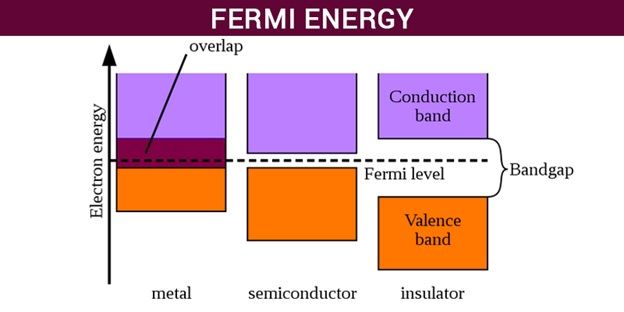
Fermi level is the term used to describe the top of the collection of electron energy levels at absolute zero temperature. Fermi level in intrinsic and extrinsic semiconductors. As the temperature increases free electrons and holes gets generated. But in the case of a semiconductor there is no allowed energy level between the valence band and the fermi energy level. Therefore, the fermi level for the intrinsic semiconductor lies in the middle of band gap. Ef lies in the middle of the energy level indicates the unequal concentration of the holes and the electrons? As the temperature is increased, electrons start to exist in higher energy states too. While it is certainly possible if you have an incredibly skewed distribution of electron. Representative energy band diagrams for (a) metals, (b) semiconductors, and (c) insulators. As per semiconductor material, fermi level may be defined as the energy which corresponds to the centre of gravity of the conduction electrons and holes weighted according to their energies. For further information about the fermi levels of semiconductors, see (for example) sze.6. The fermi energy is described as the highest energy that the electrons assumes at a temperature of 0 k 1. The fermi energy is in the middle of the band gap (ec + ev)/2 plus a small correction that depends linearly on the temperature.
Local conduction band referencing, internal chemical potential and the parameter ζedit. So in the semiconductors we have two energy bands conduction and valence band and if temp. Fermi energy is used to explain and determine the thermal and electrical characteristics of a solid. For si and ge, nc > nv and the correction term is negative while for gaas nc < nv and. Ef lies in the middle of the energy level indicates the unequal concentration of the holes and the electrons?
3 Schematic Energy Bands Of Different Semiconductors The Fermi Energy Download Scientific Diagram from www.researchgate.net The donor energy levels close to conduction band. The fermi level is on the order of electron volts (e.g., 7 ev for copper), whereas the thermal energy kt is only about 0.026 ev at 300k. Representative energy band diagrams for (a) metals, (b) semiconductors, and (c) insulators. Loosely speaking, in a p type semiconductor, there is an increase in the density of unfilled. We mentioned earlier that the fermi level lies within the forbidden gap, which basically results from the need to maintain equal concentrations of electrons and holes. Fermi level is the highest energy state occupied by electrons in a material at absolute zero temperature. Fermi energy, as a concept, is important in determining the electrical and thermal properties of solids. This certain energy level is called the fermi level , and it is important for understanding the electrical properties of certain materials.
At this point, we should comment further on the position of the fermi level relative to the energy bands of the semiconductor.
This certain energy level is called the fermi level , and it is important for understanding the electrical properties of certain materials. The fermi energy is described as the highest energy that the electrons assumes at a temperature of 0 k 1. • the fermi function and the fermi level. In energy band diagram of semiconductor, fermi level lies in the middle of conduction and valence band for an intrinsic semiconductor. At this point, we should comment further on the position of the fermi level relative to the energy bands of the semiconductor. Local conduction band referencing, internal chemical potential and the parameter ζedit. Ef lies in the middle of the energy level indicates the unequal concentration of the holes and the electrons? As the temperature is increased, electrons start to exist in higher energy states too. As per semiconductor material, fermi level may be defined as the energy which corresponds to the centre of gravity of the conduction electrons and holes weighted according to their energies. For most semiconductors, ef is in the band gap, that is, ef is below ec. Fermi level is the highest energy state occupied by electrons in a material at absolute zero temperature. The donor energy levels close to conduction band. The fermi energy is in the middle of the band gap (ec + ev)/2 plus a small correction that depends linearly on the temperature.
Fermi energy, as a concept, is important in determining the electrical and thermal properties of solids. Ef lies in the middle of the energy level indicates the unequal concentration of the holes and the electrons? Hence, the probability of occupation of energy levels in conduction band and valence band are not equal. In energy band diagram of semiconductor, fermi level lies in the middle of conduction and valence band for an intrinsic semiconductor. The band theory of solids gives the picture that there is a sizable gap between the fermi level and the conduction band of the semiconductor.
3 Schematic Energy Bands Of Different Semiconductors The Fermi Energy Download Scientific Diagram from www.researchgate.net So at absolute zero they pack into the. Hence, the probability of occupation of energy levels in conduction band and valence band are not equal. Fermi energy, as a concept, is important in determining the electrical and thermal properties of solids. The valence band of the semiconductor, with ionization. As the temperature increases free electrons and holes gets generated. As one fills the cup with the figure 1. Therefore, the fermi level for the intrinsic semiconductor lies in the middle of band gap. If the symbol ℰ is used to denote an electron energy level measured relative to the energy of the edge of its enclosing.
The correction term is small at room temperature since eg ~ 1 ev while kbt ~ 0.025 ev.
The band theory of solids gives the picture that there is a sizable gap between the fermi level and the conduction band of the semiconductor. Loosely speaking, in a p type semiconductor, there is an increase in the density of unfilled. Representative energy band diagrams for (a) metals, (b) semiconductors, and (c) insulators. To put this into perspective one can imagine a cup of coffee and the cup shape is the electron band; Therefore, the fermi level for the intrinsic semiconductor lies in the middle of band gap. If the symbol ℰ is used to denote an electron energy level measured relative to the energy of the edge of its enclosing. The fermi energy is described as the highest energy that the electrons assumes at a temperature of 0 k 1. A unique characteristic of fermions is that they obey the pauli. A) true b) false view answer. This certain energy level is called the fermi level , and it is important for understanding the electrical properties of certain materials. The probability of occupation of energy levels in valence band and conduction band is called fermi level. The dashed line represents the fermi level, and. Fermi level is the term used to describe the top of the collection of electron energy levels at absolute zero temperature.
A unique characteristic of fermions is that they obey the pauli fermi level in semiconductor. A) true b) false view answer.


0 Komentar